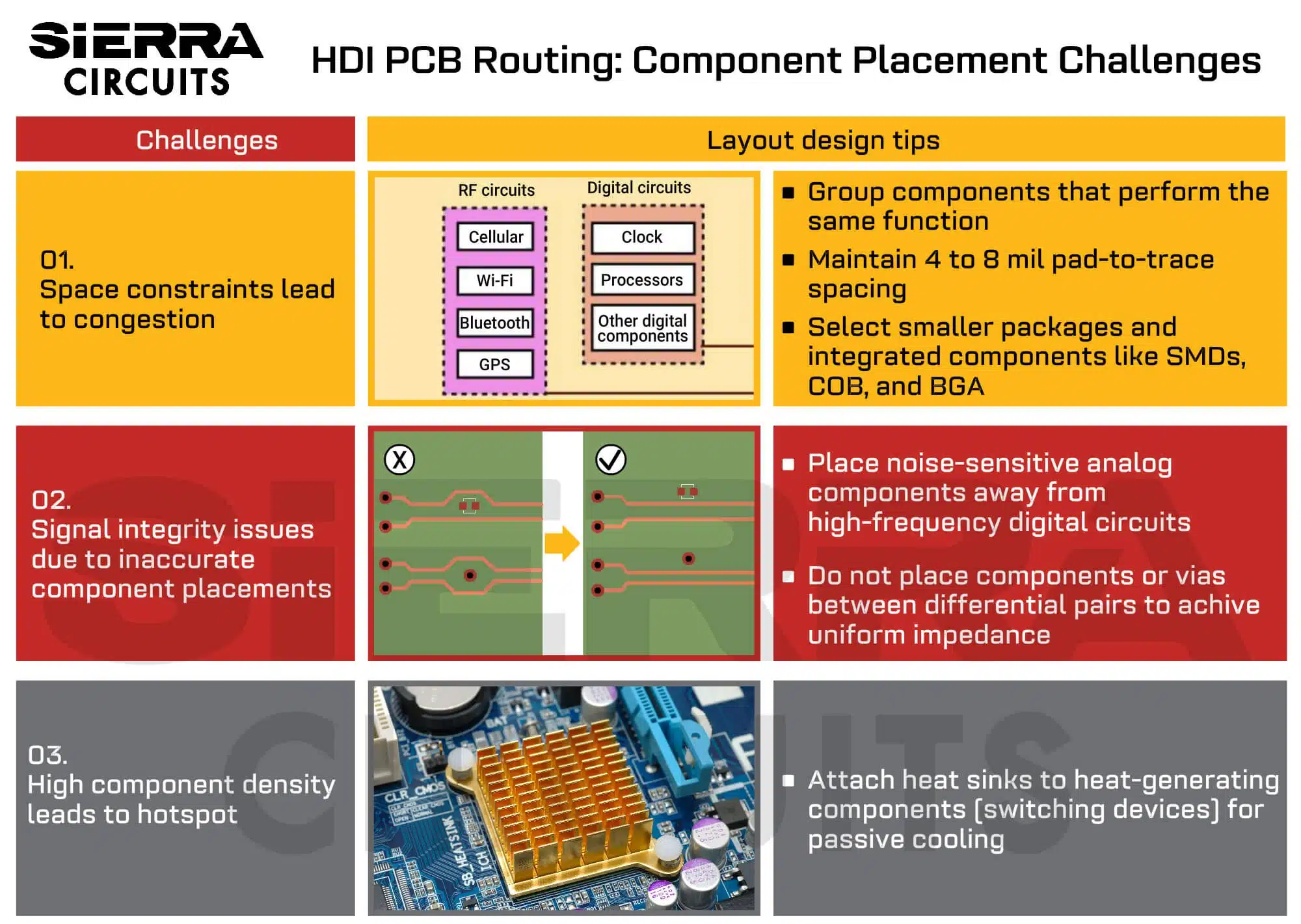
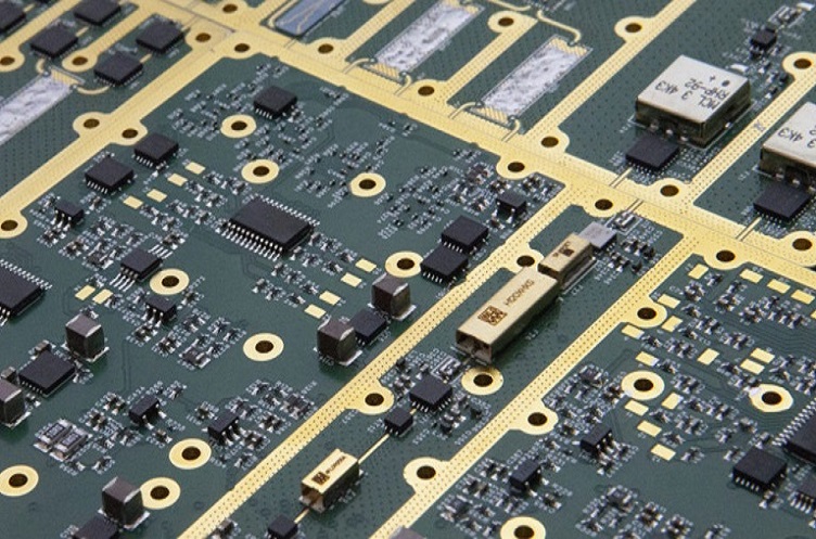
Master Electronic Engineering Using A Pcb Browser To Inspect Complex Board Traces And Component Placement Details Accurately - 5 hdi pcb routing challenges
If you are searching about PCB Component Placement Rules | Sierra Circuits you've visit to the right place. We have 35 Images about PCB Component Placement Rules | Sierra Circuits like Why We Visually Inspect Every 0201 Component Placement, What is “component placement” in PCB? - IBE Electronics and also Printed Circuit Board Assembly Services | Technical specification. Here it is:
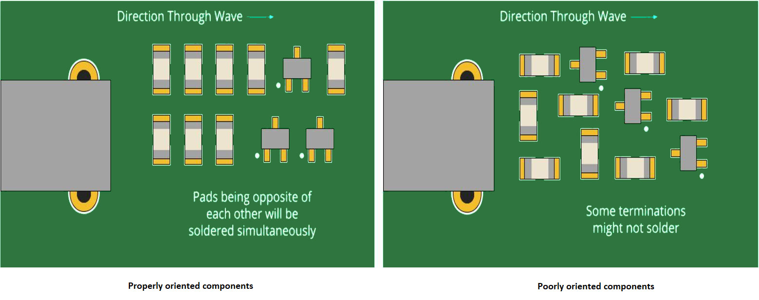
PCB Component Placement Rules | Sierra Circuits
 www.protoexpress.com
PCB Component Placement Rules | Sierra Circuits
XT1049_XT1050_XT1052_XT1053_XT1055_XT1056_XT1058_XT1060_L3_Board
 www.dzkj16888.com
XT1049_XT1050_XT1052_XT1053_XT1055_XT1056_XT1058_XT1060_L3_Board ...
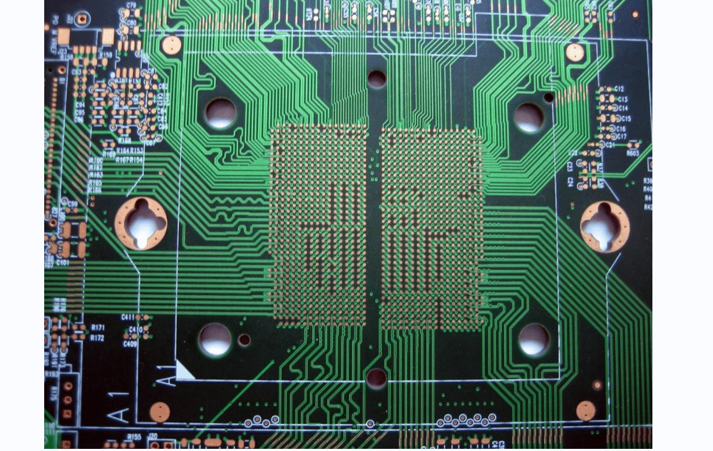
Everything You Want To Know About PCB Trace - IBE Electronics
 www.pcbaaa.com
Everything you want to know about PCB trace - IBE Electronics
Hf6a0753 Stock Illustrations – 1 Hf6a0753 Stock Illustrations, Vectors
 www.dreamstime.com
Hf6a0753 Stock Illustrations – 1 Hf6a0753 Stock Illustrations, Vectors ...
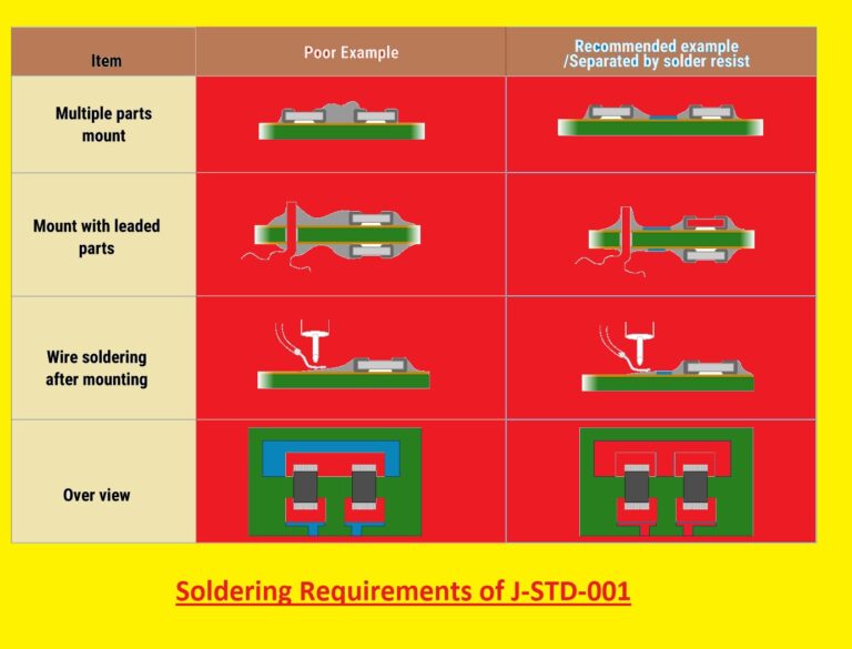
J-STD-001| J Standard Soldering Requirements - The Engineering Knowledge
 www.theengineeringknowledge.com
J-STD-001| J Standard Soldering Requirements - The Engineering Knowledge
Detailed CloseUp Of A Modern Electronic Printed Circuit Board PCB On A
 www.dreamstime.com
Detailed CloseUp of a Modern Electronic Printed Circuit Board PCB on a ...
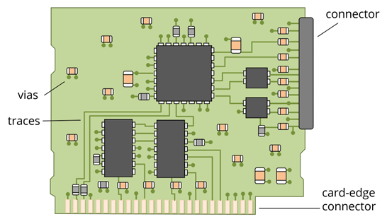
What Is “component Placement” In PCB? - IBE Electronics
 www.pcbaaa.com
What is “component placement” in PCB? - IBE Electronics
Complex PCB Design: Tips And Best Practices For Successful
 hillmancurtis.com
Complex PCB Design: Tips and Best Practices for Successful ...
PCB Tombstone: 9 Ways To Avoid It?
 www.fscircuits.com
PCB Tombstone: 9 Ways to Avoid It?
What Is High Frequency PCB ? – GREATPCB
 greatpcb.com
What is High Frequency PCB ? – GREATPCB
What Is A PCB Symbol? - RayPCB
 www.raypcb.com
What is a PCB Symbol? - RayPCB
Inspect Tool In Microsoft Edge Browser - GeeksforGeeks
 www.geeksforgeeks.org
Inspect Tool in Microsoft Edge Browser - GeeksforGeeks
RF PCB And Its Design Guidelines - Fx PCB
 sfxpcb.com
RF PCB and Its Design Guidelines - Fx PCB
Technical Macro Of A Gold Contact On A PCB Stock Illustration
 www.dreamstime.com
Technical Macro of a Gold Contact on a PCB Stock Illustration ...
Intricate Blue Circuit Board Macro A Stunning Deep Dive Into Futuristic
 www.dreamstime.com
Intricate Blue Circuit Board Macro a Stunning Deep Dive into Futuristic ...
Comprehensive Technical Drawing Of A Detailed Printed Circuit Board
 www.dreamstime.com
Comprehensive Technical Drawing of a Detailed Printed Circuit Board ...
Detailed HighDepthofField PCB Design CAD Drawing Precise Conductors
 www.dreamstime.com
Detailed HighDepthofField PCB Design CAD Drawing Precise Conductors ...
PCB Soldering Basics: Techniques, Types, And Tools Explained
 www.fastturnpcbs.com
PCB Soldering Basics: Techniques, Types, And Tools Explained
Design A PCB Layout Showing Component Placement And Copper Traces
 www.freepik.com
Design a PCB layout showing component placement and copper traces ...
Component Placement: The Importance Of Proper Placement For PCB Design
 blogs.sw.siemens.com
Component Placement: The Importance of Proper Placement for PCB Design ...
How Any Layer HDI PCB Offer Interconnect Solution To Complex Electronic
 hillmancurtis.com
How Any Layer HDI PCB Offer Interconnect Solution to Complex Electronic ...
Detailed Circuit Board Layout Schematic Displaying Accurate Positioning
 www.dreamstime.com
Detailed Circuit Board Layout Schematic Displaying Accurate Positioning ...
LearnEMC - PCB Layout
 learnemc.com
LearnEMC - PCB Layout
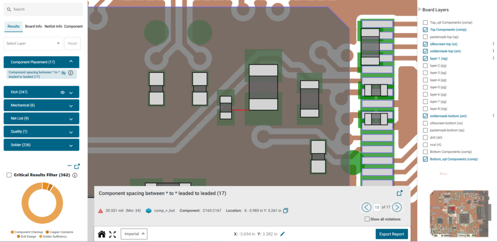
5 HDI PCB Routing Challenges | Sierra Circuits
 www.protoexpress.com
5 HDI PCB Routing Challenges | Sierra Circuits
Burnt Smd Parts Stock Photos - Free & Royalty-Free Stock Photos From
 www.dreamstime.com
Burnt Smd Parts Stock Photos - Free & Royalty-Free Stock Photos from ...
The Essentials Of Solder Joints : A Comprehensive Guide - Mainpcba One
 www.mainpcba.com
The Essentials of Solder Joints : A Comprehensive Guide - Mainpcba One ...
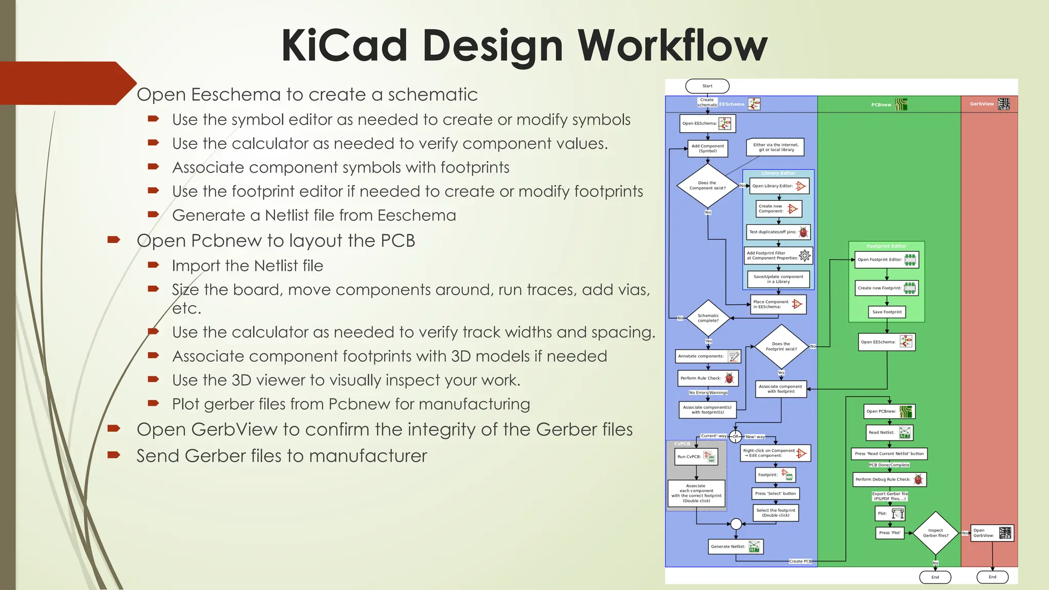
PCB_Design_with_KiCad_Buvana_Rev3.ppt Ece | PPTX
 www.slideshare.net
PCB_Design_with_KiCad_Buvana_Rev3.ppt ece | PPTX
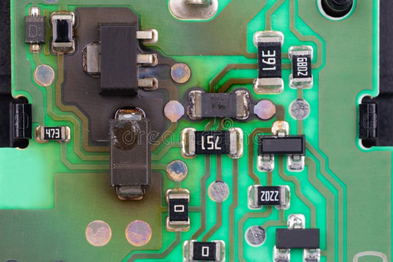
Why We Visually Inspect Every 0201 Component Placement
 electroniccomponent.com
Why We Visually Inspect Every 0201 Component Placement
PCB Tombstone: Understanding, Prevention And Effects On PCB
 www.pcbmay.com
PCB Tombstone: Understanding, Prevention and Effects on PCB
Component Placement Rules For Surface Mount Technology (SMT)
 www.allpcb.com
Component Placement Rules for Surface Mount Technology (SMT)
What Is A Netlist? Understanding The Basics Of Electronic Design Automation
 www.flux.ai
What Is a Netlist? Understanding the Basics of Electronic Design Automation
Printed Circuit Board Assembly Services | Technical Specification
 www.hemeixinpcb.com
Printed Circuit Board Assembly Services | Technical specification
Unveiling The Intricate Microcosm Of Electronic Circuitry A Microscopic
 www.dreamstime.com
Unveiling the Intricate Microcosm of Electronic Circuitry a Microscopic ...
PCB Design Process | Key Steps For Efficient Circuit Board Development
 www.slideshare.net
PCB Design Process | Key Steps for Efficient Circuit Board Development ...
PCB Prepreg: A Comprehensive Guide - MorePCB
 morepcb.com
PCB Prepreg: A Comprehensive Guide - MorePCB
Why we visually inspect every 0201 component placement. Intricate blue circuit board macro a stunning deep dive into futuristic. pcb_design_with_kicad_buvana_rev3.ppt ece